

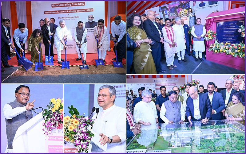
Groundbreaking of India’s First Advanced 3D Semiconductor Packaging Unit in Odisha
20 April 2026: In a defining moment for India’s semiconductor ambitions and Odisha’s emergence as a future-ready technology destination, the foundation stone for the country’s first advanced 3D chip packaging unit was laid today at Info Valley, Bhubaneswar. Project marks a significant step towards strengthening India’s domestic semiconductor ecosystem and advancing the vision of Atmanirbhar Bharat in high-end electronics manufacturing.
The foundation stone of the Heterogeneous Integration Packaging Solutions project, promoted by 3D Glass Solutions, was laid in the presence of Chief Minister Mohan Charan Majhi and Union Minister for Railways, Electronics & Information Technology, and Information & Broadcasting Ashwini Vaishnaw. With the launch of this project, Odisha is poised to become home to one of the world’s most sophisticated chip packaging technologies.
Addressing the gathering, Chief Minister Mohan Charan Majhi described the project as a historic milestone for Odisha and the nation. He said that for the first time in India, an advanced 3D Glass Solutions semiconductor project is being established, bringing immense pride to the state. He noted that global technology leaders such as Intel, Lockheed Martin, and Applied Materials are associated with cutting-edge packaging technologies and their interest in Odisha reflects the state’s growing industrial strength.
Majhi informed that the company is investing nearly Rs.2,000 crore in the project and the facility is expected to produce 70,000 glass panels annually, along with 50 million assembled units and around 13,000 advanced 3DHI modules. He added that Odisha has emerged as the only state in the country where both India’s first compound semiconductor fabrication unit and first 3D glass substrate packaging facility are being established.
Addessing the gathering, Union Minister Ashwini Vaishnaw congratulated the people of Odisha on the landmark initiative and appreciated the support extended by the State Government. He said, under the visionary leadership of Prime Minister Shri Narendra Modi, India’s semiconductor sector is witnessing rapid growth, with Odisha emerging as an important contributor to this transformation.
Vaishnaw said, Odisha, traditionally known for its strengths in minerals, metals and energy, is now steadily establishing itself in advanced sectors such as electronics, IT and semiconductors. Describing the project as one of the most advanced manufacturing initiatives of its kind, he said it would significantly strengthen India’s semiconductor value chain.
He further informed that two semiconductor projects have already been approved for Odisha under the India Semiconductor Mission, while three more electronics and semiconductor-related proposals are in the pipeline. “Discussions are also underway with major global companies, including Intel for future investments in the state,” he mentioned.
State Minister for Electronics & IT, Dr. Mukesh Mahaling, said Odisha is fast emerging as a semiconductor hub, with two approved projects under the India Semiconductor Mission, including the advanced 3D Glass unit inaugurated today. He said the State Government’s IT, AI, GCC and Semiconductor Policies 2025 will drive innovation and attract investments. Emphasising skill development, he said stipend support for engineering students is being provided to build an industry-ready workforce. He added that initiatives like the Blackswan Summit 2026 and growing AI investments will create jobs and strengthen Odisha’s leadership in future technologies.
Project is being implemented by 3D Glass Solutions Inc. (3DGS), USA, through its wholly owned Indian subsidiary Heterogeneous Integration Packaging Solutions (P) Ltd. (HIPSPL) at Info Valley in Khordha district. It is a greenfield, vertically integrated advanced packaging and embedded glass substrate ATMP facility. Total investment in the project is Rs.1,943.53 crore, including approved Central fiscal support of Rs.799 crore and additional State support of approximately Rs.399.5 crore.