


MicroCraft Introduces Super Large Format High-Speed Inkjet Printer for PCBs
18 January 2022: During the recently concluded electronica India/IPCA Expo in Bengaluru, Japan-based MicroCraft KK digitally showcased their high speed, super large format inkjet digital printing system – model CPi 120110 – for Printed Circuit Boards (PCBs). The printer is capable of printing extremely large size PCBs (48×44 inch/45×35.8 inch and 45×31.1 inch). During the 3-day exhibition, the TV screen at their stall was also displaying MicroCraft’s CraftPix series digital printers, said to be the industry’s first on-demand inkjet printing system.
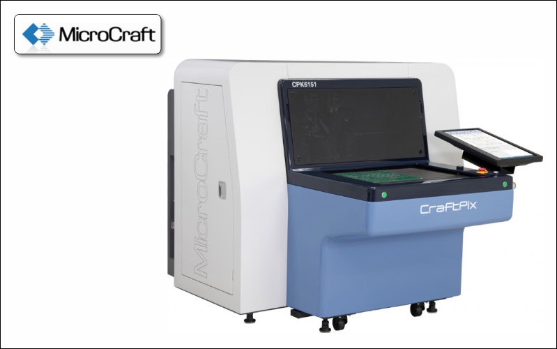
MicroCraft, with its India regional office in Bengaluru, offers right from super high speed to high speed to medium speed models (standard and budget models, dual ink printing models, small ink quantity models). CraftPix is a UV curable inkjet printer that is capable of printing images directly onto the target material with precise accuracy. The digital system is fitted with a UV curing lamp for high speed and immediate curing and there is no need for an offline UV curing machine.
Our CraftPix series digital printers bypass the conventional production process to achieve improved print quality, reduced costs and reduced environmental impact,” says Sanjay Singh, Sales Engineer, MicroCraft India, adding, “the inkjet printer offers a speedy digital process of printing legends, solder resist, and nameplates. And film and stencil making can now be thing of the past. Moreover, the drop on demand inkjet printer allows uneven surface printing which is not possible with conventional silk screen printing.”
He adds “With the fully digitized printing process, operators gain greater flexibility as small changes and corrections can be made to the print job even at the last minute. Equipment such as squeegees, screens, exposure machines and even some chemical solutions that were required in the conventional process is no longer required. In addition, the elimination of UV exposure in the production line helps improve productivity.”
Sanjay Singh says that the digital printing system does not involve the use of solvents, thus reducing the risk of environmental pollution. The automatic ink recycling system equipped with CraftPix also contributes to environmental protection and cost savings.
Traditionally screen printing process was used in PCB production. For e.g in the traditional screen printing the steps involves: For Side A, screen creation, alignment, screen printing, heat curing and screen cleaning, and repeat the same steps for Side B. Digitalisation of the PCB printing, on the other hand, data is loaded, side A is printed, side B is printed and heat curing is done instantly.
Similarly, in the solder resist image printing, doing manual alignment of the photo tool without any error is a difficult task and application of solder resist ink in QFP open area remains a big challenge. The steps involve flood coating of mask panel, oven tack curing, setting up mask photo-tool, UV exposure and development. On the other hand, with the digital process, solder resist can be applied more accurately involving direct printing of solder resist, followed by final curing.
And, to form flexible PCB’s cover-lay with inkjet printing, one has to just apply solder resist and heat cure, thus requiring shortened fabrication procedures with more accurate and speedy printing. Whereas in the conventional process, one has to do cover-lay punch, apply adhesive, attach cover-lay, apply photosensitive solder resist, dry, expose, develop and heat cure, thus production cost is high in the conventional process due to several steps.
Moreover, with digital, the process of etching nameplates and marking nameplates is easier. CraftPix prints etch resist ink directly onto the metal substrate such as aluminium and stainless and it is capable of applying ink into cavity fill once the printing process is completed. Marking ink can also be directly printed onto the metal substrate. The conventional method involves the use of stencil and squeegee, and many long processes thus requiring a lot of time and money. It involves screen creation, alignment, applying to etch resist ink, curing/baking, etching, peeling etch resist ink, screen cleaning and storage and for cavity fill it involves paint booth/spray flood, oven bake, washing and polishing and drying.
singh@microcraft-india.com