


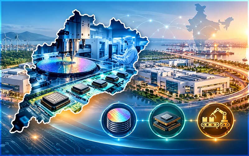
Odisha Semiconductor Ecosystem Takes Shape Around Chipmaking and Packaging
25 September 2026: Odisha’s semiconductor ambitions gained a concrete project milestone at Info Valley, Bhubaneswar, with a foundation-stone ceremony for a 3D Glass Solutions packaging facility, reported on 20 April 2026. The development gives the Odisha semiconductor ecosystem a specific industrial focus, although a groundbreaking does not establish that commercial production has begun.
What is shaping the Odisha semiconductor ecosystem?
Screen Print India’s Odisha packaging project report identifies the developer as Heterogeneous Integration Packaging Solutions, the Indian subsidiary of US-based 3D Glass Solutions. The report places the project at Info Valley in Khordha district and describes a planned advanced-packaging and embedded-glass-substrate facility.
The distinction between chipmaking and packaging matters. 3D Glass Solutions describes its technology as glass substrates and three-dimensional heterogeneous integration for semiconductor packaging.
Separately, SiCSem’s company website sets out plans for silicon carbide manufacturing covering crystal growth, device fabrication, assembly and testing. The company identifies diodes, MOSFETs and power modules as its products, with intended applications including electric vehicles, chargers and renewable-energy systems.
Industrial strengths are a starting point
Odisha’s investment-promotion agency lists electronic system design and manufacturing among its focus sectors for investment, alongside chemicals, downstream metal industries and technical textiles. These priorities explain the state’s interest in building a broader supplier base around semiconductor projects. Reliable utilities, suitable facilities and trained workers remain practical priorities.
Where could printing companies participate?
For industrial printers, the brief’s proposed opportunities in functional inks, substrates, sensors and electronic interfaces deserve investigation.
Screen Print India’s coverage of printed electronics in textiles illustrates an adjacent application area. It does not establish that textile printing, conventional graphics production or wearable electronics share the same qualification requirements as semiconductor fabrication.
Skills must develop alongside facilities
The workforce discussion also extends beyond engineers. Screen Print India’s report on the proposed India Semiconductor Academy describes plans covering technicians, equipment operators, manufacturing engineers and materials scientists, with practical training in facilities, maintenance, packaging and testing.
That national proposal offers relevant context, but it is not evidence of an operating training programme dedicated to Odisha’s projects. Local education and industry partnerships will need to connect training with identifiable roles and employer requirements.
This creates opportunities for Indian SMEs and technology companies to become part of the emerging supply chain. Industrial screen printing and functional printing, for example, can support applications involving conductive materials, electronic interfaces, labels, membranes, sensors and other specialised components.
The continuing flow of private capital, alongside government initiatives supporting semiconductor manufacturing and technology development, suggests that India’s semiconductor story is moving beyond policy ambition towards ecosystem building. The challenge now will be to broaden investment across more companies, develop specialised talent and build globally competitive supply chains capable of supporting sustained semiconductor manufacturing and innovation in India.

Sorry, the comment form is closed at this time.